Actualités


17 avril 2024
Fin de session et recherche de stage


11 avril 2024
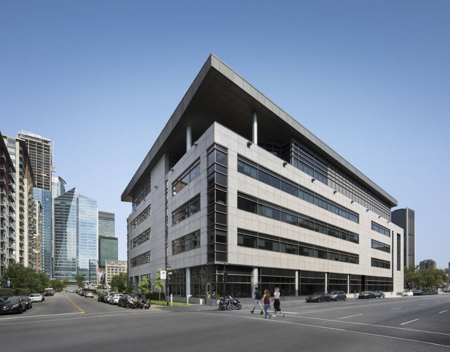
L’ÉTS accueillera la 92ᵉ édition du Congrès de l’Acfas avec la collaboration de l’Université Concordia

11 avril 2024
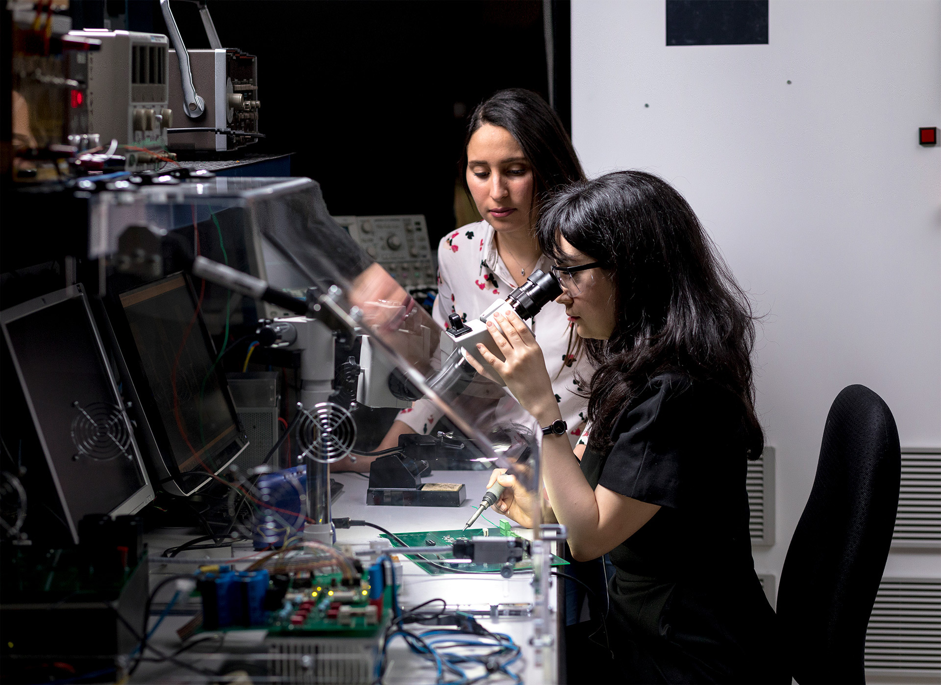
Journée francophone des femmes en informatique


1
Vous êtes actuellement sur cette page
2
Aller à la page : 2
3
Aller à la page : 3
...
51
Aller à la page : 51
Aller à la page suivante
Explorez votre avenir
universitaire